
In the rapidly evolving landscape of industrial electronics—spanning AI, medical equipment, and automotive control systems—the demand for miniaturization and high performance is non-negotiable. As a veteran in the industry, I have witnessed the transition from simple double-sided boards to complex high-density interconnects. At the heart of this evolution lies a critical, often overlooked component: the Multilayer PCB Vias.
At Yichao Quick Technology Co., Ltd, we understand that a via is not just a hole; it is the vital conduit that ensures electrical continuity and thermal management across up to 64 layers of circuitry. This guide explores the technical anatomy, diverse types, and advanced processing methods of PCB vias, demonstrating why precision manufacturing is essential for your B2B applications.
1. What is a PCB Via? The Foundation of Interconnectivity
A “Via” (Vertical Interconnect Access) is a copper-plated hole that creates an electrical connection between different layers of a printed circuit board. In the realm of Multilayer PCB Vias, these microscopic tunnels allow signals and power to traverse the Z-axis of the board, transforming a stack of insulating and conductive materials into a functioning three-dimensional circuit. Without robust vias, the complex routing required for modern microprocessors and FPGA chips would be impossible.
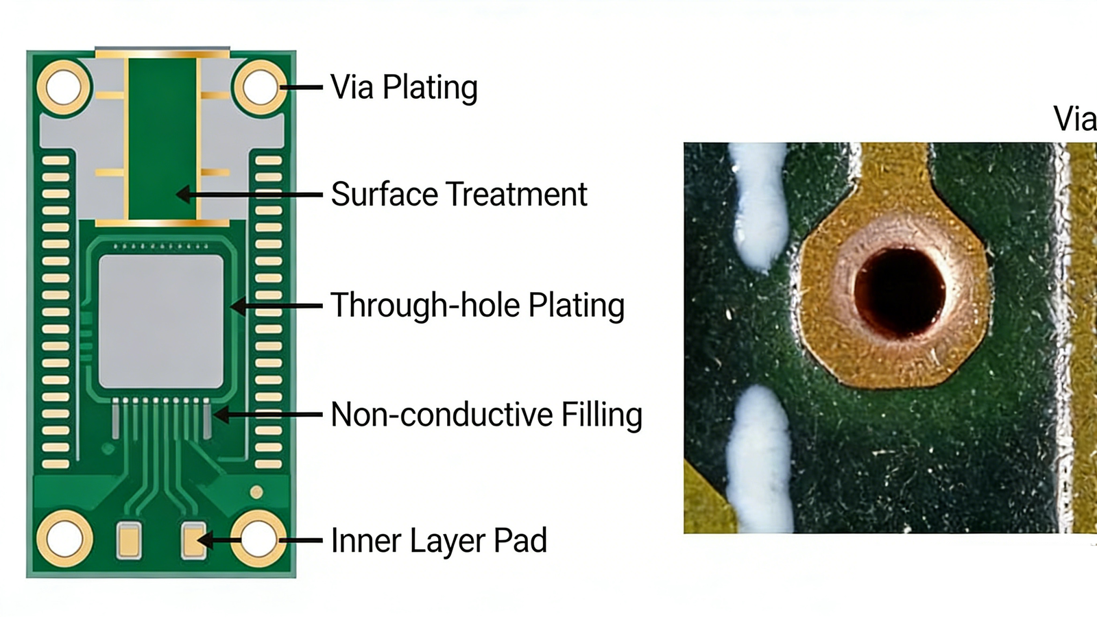
2. The Anatomy of a Via: Composition and Structure
To evaluate quality, procurement managers and engineers must understand the composition of a via. A standard via consists of three main components:
- The Barrel: This is the conductive tube filling the drilled hole. At Yichao, we utilize advanced electroplating lines to ensure the copper wall thickness meets strict IPC standards, ensuring durability under thermal cycling.
- The Pad: The metal ring on the surface of each layer that connects the barrel to the component or circuit trace.
- The Antipad: A clearance hole in the metal layers that the via passes through without connecting, preventing short circuits in power or ground planes.
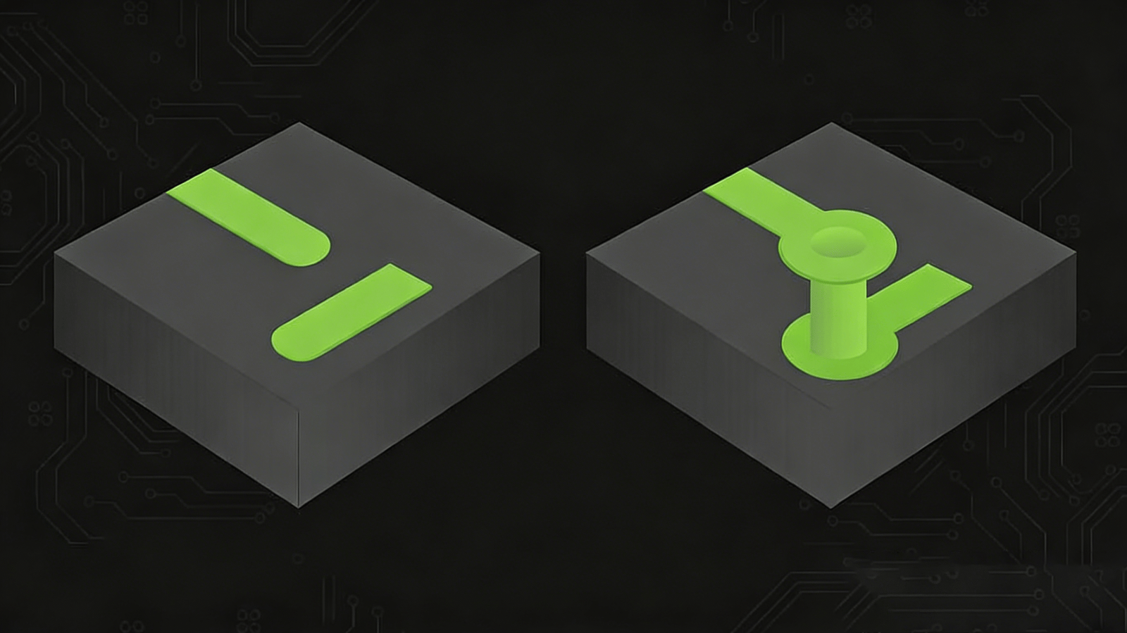
3. Classifying PCB Via Types: From Standard to High-Density
Different applications require specific interconnect strategies. We offer a comprehensive range of PCB Via Types tailored to various density and signal requirements.
Plated Through-Hole (PTH) Vias
The most common type, passing through the entire board from the top layer to the bottom layer. While cost-effective, they consume valuable routing space on layers where they aren’t electrically connected.
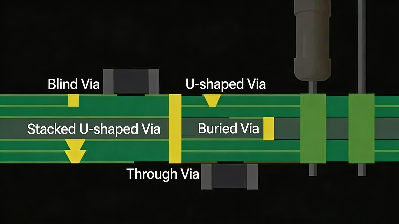
Blind Vias
Blind vias connect an outer layer to one or more inner layers but do not go through the entire board. They are visible from only one side. This technology is crucial for High-Density Interconnect (HDI) designs, freeing up space on the opposite side for other components.
Buried Vias
Buried vias connect two or more inner layers and are completely invisible from the outer layers. These are drilled and plated in the inner core stages before the final lamination. They are essential for complex routing in high-layer-count boards, such as those used in telecommunications.
Microvias
Microvias are minute holes (usually less than 0.15mm in diameter) drilled using lasers. They are predominantly used in HDI boards to connect adjacent layers. Yichao utilizes internationally advanced LDI exposure machines and laser drills to achieve the precision required for microvias.
Via-in-Pad Technology
For components with extremely tight pitches, such as BGAs (Ball Grid Arrays), standard “dog-bone” routing is insufficient. Via-in-Pad Technology places the via directly under the component’s solder pad. The via is then filled (with resin or copper) and capped (plated over) to create a flat surface. This technique significantly reduces inductance and saves board real estate.
4. The Critical Functions of PCB Vias
Vias serve more than just a connective purpose; they are functional powerhouses in PCB design:
- Signal Routing: They enable the complex crisscross of signals required in multilayer boards, ensuring signals reach their destination with minimal interference.
- Power Delivery: Large arrays of vias often connect power and ground planes, ensuring stable voltage delivery to power-hungry ICs.
- Thermal Management: Thermal vias transfer heat away from hot components (like power amplifiers or processors) to the other side of the board or into inner copper planes, acting as heat pipes. This is vital for the reliability of industrial control and new energy equipment.
5. Advanced Via Processing Technology at Yichao
The reliability of a via is determined by the manufacturing process. At Yichao Quick Technology, we adhere to strict quality controls (ISO9001, IATF16949) to ensure every via performs flawlessly.
Drilling Precision: We employ DaZu six-axis drilling machines for mechanical drilling and advanced laser systems for microvias. This ensures positional accuracy and clean hole walls, preventing defects like smear that can disrupt connectivity.
Desmear and Plating: Before plating, we perform chemical desmearing to remove resin residues caused by drilling heat. Our automated copper sinking and electroplating lines deposit a uniform layer of copper. For Via-in-Pad Technology, we utilize specialized plugging processes (resin plug + copper cap) to ensure a perfectly flat surface for soldering, eliminating the risk of air bubbles or solder wicking.
Conclusion: Why Partner with Yichao for High-Complexity PCBs?
In the world of high-end manufacturing, the integrity of your product relies on the quality of its connections. Whether you require standard through-holes or complex HDI boards with blind and buried vias, the processing method matters.
Yichao Quick Technology combines over a decade of industry expertise with state-of-the-art equipment to deliver reliable, high-performance PCB solutions. With our ability to support up to 64 layers and deliver prototypes in as fast as 24 hours, we are the strategic partner you need to bring your innovations to market. Contact us today to discuss how our advanced via technologies can optimize your next project.