A team of 50+ senior engineers. We provide one-stop service from
design to mass production.
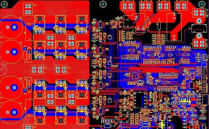
PCB design + PCB manufacturing + SMT assembly + stencil manufacturing + BOM sourcing: a one-stop service.
≤42-layer
≥2MIL(HDI)
≤110000+
≥2MIL(HDI)
≥0.2mm
≤2912
≤60GHZ
78000+
[≤1000 PINs] 3-5 days, [≥8000 PINs] 15-18 days, [≥16000 PINs] 22-30 days
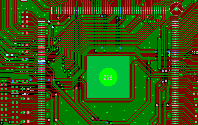
5G high-speed PCIe differential routing
6-layer RK3288 tablet PC
Industrial control board
RF antenna processing
Blind buried hole cable outlet
Schematic diagram (schdoc, DSN, or sch), netlist, structural diagram (DXF), component library (datasheet required for newly created components), design requirements, etc.
This review is conducted according to design specifications, design guidelines, customer design requirements, and relevant checklists. After project initiation, our engineers perform schematic DRC checks, structural verification, and other electrical design requirements. Any issues are immediately reported to the customer via EQ records.
Provide layout and structural files for customer review; the customer confirms the rationality of the layout, stacking scheme, impedance scheme, structure, and packaging, and confirms the routing parameters.
PCB source files, Gerber files, assembly files, stencil files, structural files, etc. After the PCB layout design is completed, our engineers will perform cross-checks, including DFM checks, QA checks, and EMC checks. Once the customer confirms everything is OK, we will generate Gerber and other production files.

6-layer RK3288 set-top box project