
In the high-stakes world of industrial electronics, the distance between a functional concept and a market-ready product is often measured in manufacturing precision. For decades, I have watched brilliant engineering designs falter not because of bad logic, but due to a lack of understanding regarding the physical manufacturing process. Whether you are developing AI hardware, medical equipment, or industrial control systems, bridging the gap between digital files and physical boards is critical. This PCB Design to Production Guide is crafted to help you navigate that journey seamlessly, leveraging professional manufacturing standards.
1. The Foundation: Component Selection and Packaging Strategy
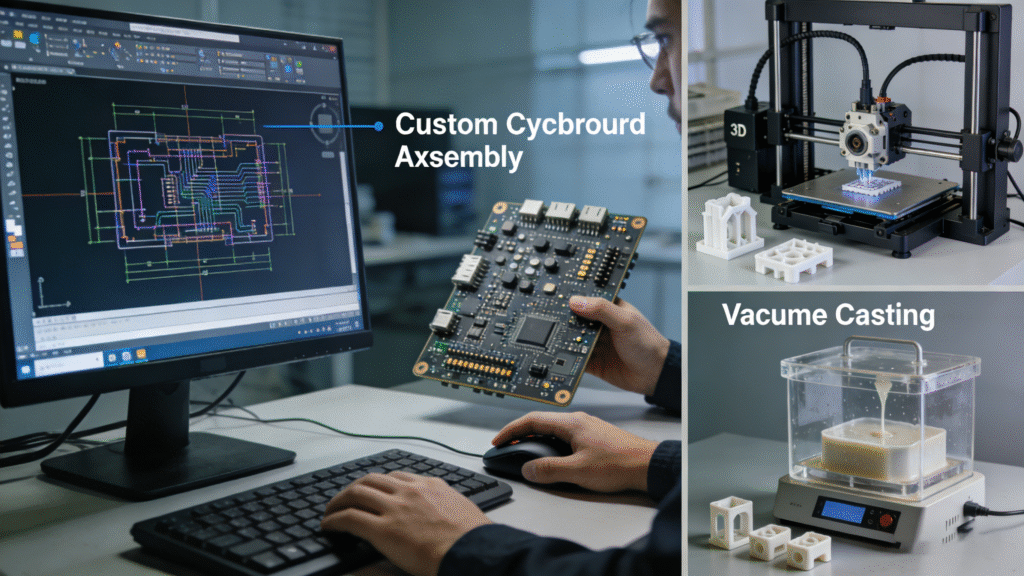
Before a single trace is routed, the success of your project hinges on component selection. In our experience at Yichao, manufacturing delays often stem from mismatched package types or obsolete components. Understanding the physical footprint—the “package”—is the first step in Design for Manufacturing (DFM).
We typically categorize packages into through-hole (DIP) and Surface Mount Technology (SMT). For modern, high-density applications, SMT is the standard. You will encounter:
- SOP/SOIC (Small Outline Package): A staple for integrated circuits.
- QFP/QFN (Quad Flat Package): Essential for microcontrollers, with QFN offering better thermal performance due to the exposed pad.
- BGA (Ball Grid Array): Critical for high-performance processors. Note that BGA requires precise X-Ray inspection during manufacturing, a standard protocol in our facilities.
Furthermore, understanding passive component sizing is vital. The jump from an 0603 to an 0402 resistor might seem trivial on a screen, but it impacts assembly density and power handling. We recommend consulting with your Custom PCB Assembly Services provider early to ensure your chosen components are stock-available and machine-compatible.
2. Power Architecture: Stability Starts Here
A circuit board is only as reliable as its power delivery network. In industrial applications, where equipment operates 24/7, power design is not just about voltage—it is about thermal management and noise suppression.
Designers generally face a choice between Linear Regulators (LDOs) and Switching Power Supplies. LDOs offer low noise and simplicity but can generate significant heat if the voltage drop is high. Switching supplies (Buck/Boost converters) offer high efficiency but introduce ripple. For high-reliability boards, proper filtering—using capacitors and ferrite beads (magnetic beads)—is non-negotiable to suppress high-frequency noise. Ensuring your design has robust power planes is a key aspect of our High-Reliability Circuit Board Design philosophy.
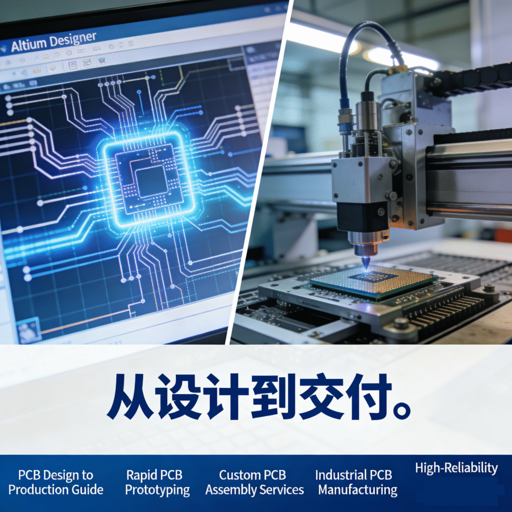
3. From Schematic to Layout: The Design Process
Transitioning from schematic to PCB layout requires a disciplined workflow. The use of professional tools like Altium Designer allows for the integration of 3D models, which is a game-changer for avoiding mechanical collisions in the final enclosure.
Creating Accurate Libraries
Never assume a downloaded footprint is correct. Verify component datasheets against your layout library. At Yichao, we see numerous projects stalled because a custom connector’s footprint didn’t match the physical part. Building a validated library is an investment in speed.
Routing for Signal Integrity
When routing, consider the physical behavior of electricity. Key rules include:
- Trace Width: Standard signal lines often use 10-12 mil, while power lines must be significantly wider (30-50 mil) to handle current without overheating.
- Avoid Right Angles: Acute or 90-degree angles can cause acid traps during etching and impedance discontinuities. 45-degree routing is the professional standard.
- Loop Area: Minimize the loop area for signals, especially high-frequency ones, to reduce electromagnetic interference (EMI).
4. The Manufacturing Leap: Prototyping and Assembly
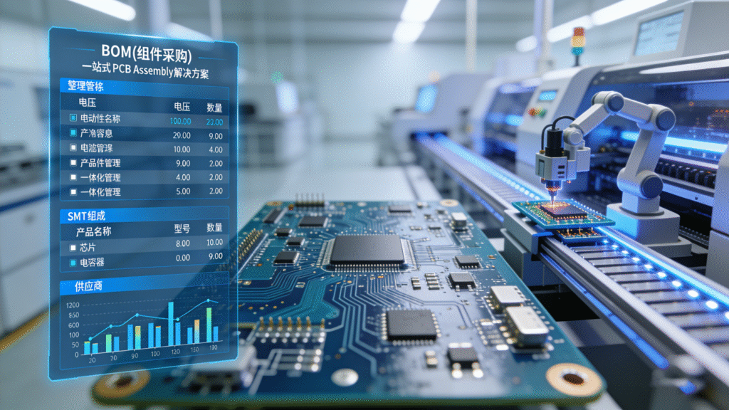
Once your design passes the DRC (Design Rule Check), the focus shifts to fabrication. This is where partnering with a specialized manufacturer transforms your file into a product. This stage is often referred to as Rapid PCB Prototyping.
Speed and precision are paramount. At Yichao, we leverage “Specialized, Refined, and Innovative” manufacturing methodologies. Our automated lines can handle everything from complex HDI blind/buried via boards to rigid-flex combinations. The advantage of a one-stop solution is that we manage the component sourcing (BOM) and the SMT assembly simultaneously. This integrated approach allows us to achieve ordering-to-shipping times as fast as 12 hours for urgent projects.
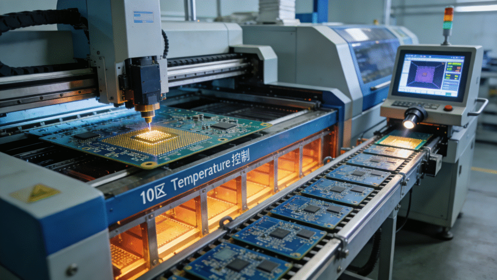
5. Why Professional Assembly Matters
While DIY soldering is an educational rite of passage, professional B2B applications require industrial-grade SMT assembly. Features like solder paste stencil printing, reflow soldering with 10-zone temperature control, and AOI (Automated Optical Inspection) ensure that every one of the millions of solder points we process daily meets ISO9001 and IATF16949 standards.
Whether you are utilizing Rogers materials for high-frequency communication or heavy copper for power electronics, the manufacturing process must align with the design intent. By collaborating with a partner that understands both the engineering and the execution, you ensure your product is not just designed well, but built to last.
Conclusion
Mastering the PCB design process is a journey of continuous learning. By adhering to strict design rules and partnering with a capable manufacturer like Yichao, you can ensure your innovations move smoothly from the screen to the real world.