
In the rapidly evolving landscape of industrial electronics, the demand is clear: smaller, faster, and more powerful. As an industry veteran who has watched circuit boards evolve from simple single-sided panels to complex multi-layer architectures, I can tell you that HDI PCB (High Density Interconnect Printed Circuit Board) is not just a trend—it is the standard for modern high-end manufacturing.
For product engineers and procurement managers, understanding HDI is crucial. It is the technology that allows us to pack the processing power of a supercomputer into a handheld device or a critical medical instrument. At Yichao Quick Technology Co., Ltd, we have refined our manufacturing processes over the last decade to master this complexity, ensuring that your most ambitious designs become reliable realities.
Defining the Core: What Exactly is HDI?
At its simplest definition, an HDI PCB is a circuit board with a much higher wiring density per unit area than conventional PCBs. But the definition goes deeper than just density. It represents a paradigm shift in manufacturing methodology.
Unlike traditional boards that rely on mechanically drilled through-holes, HDI boards utilize advanced laser drilling technology, fine lines, and high-performance materials. This technology facilitates the connection of components in incredibly tight spaces, supporting the high pin-count demands of modern ICs and processors.
The Technical Pillars of HDI Manufacturing
To truly appreciate the value of an HDI board, one must look under the surface. The superiority of High Density Interconnect PCB technology rests on three specific technical pillars that we rigorously control at our Shenzhen facility:
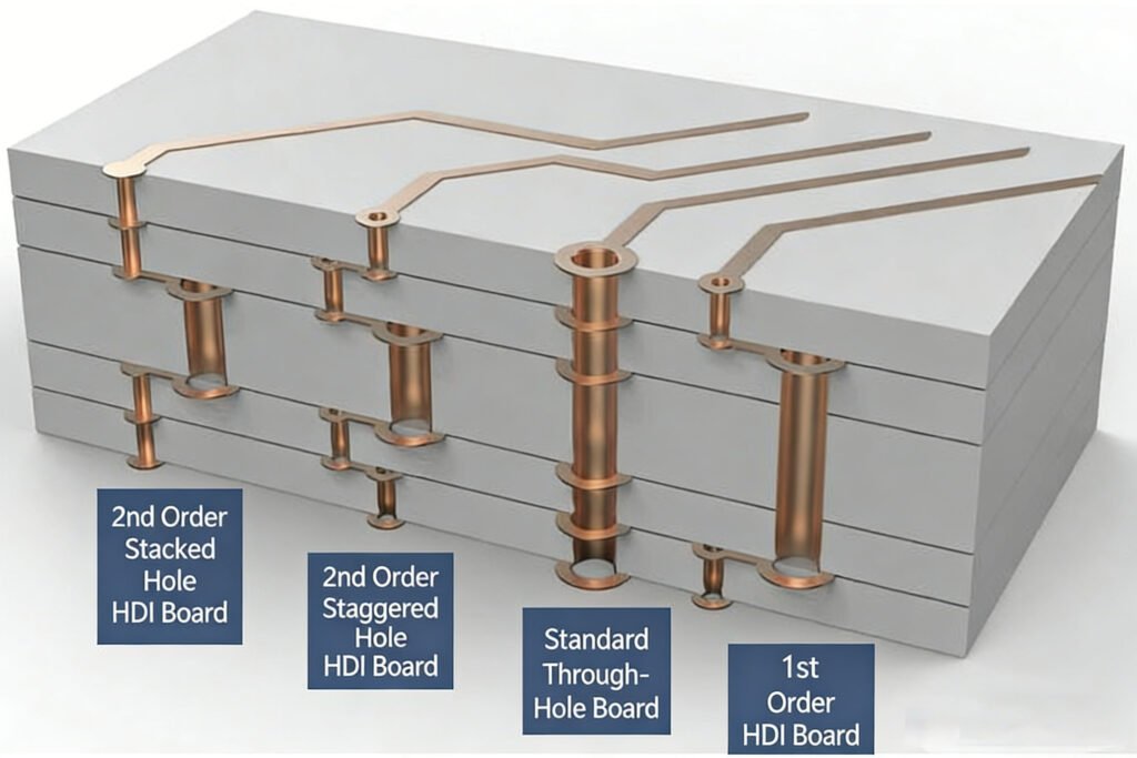
1. Microvia Technology
The heart of HDI is the microvia. These are laser-drilled holes with a diameter typically less than 150 microns (6 mils). Because they are created using lasers rather than mechanical drill bits, they are incredibly precise. At Yichao, we utilize internationally advanced LDI exposure machines and laser drills to ensure perfect registration. These microvias allow for tighter pad placement, freeing up valuable real estate on the board surface for more components.
2. Blind and Buried Vias
In a standard PCB, a hole often goes all the way through the board. In HDI, we use blind vias (connecting an outer layer to an inner layer without going through the entire board) and buried vias (connecting inner layers only). This complex routing capability means we can create “highways” for electrical signals inside the board without congesting the surface. This is essential for boards supporting up to 40 layers—a capability Yichao is proud to offer.
3. Sequential Lamination Cycles
Building an HDI board is like constructing a skyscraper floor by floor. We don’t just press all layers at once; we build them up sequentially. This process requires precise control over heat and pressure to ensure structural integrity. Our factory operates with strict adherence to ISO9001:2015 and IATF16949 standards to manage these complex lamination cycles, preventing delamination and ensuring long-term reliability.
Why Shift to HDI? The Strategic Advantages
For B2B buyers in sectors like industrial control or AI, switching to HDI PCB designs offers tangible competitive edges:
- Miniaturization: You can reduce the physical size and weight of your device without sacrificing performance. This is critical for portable medical devices and aerospace applications.
- Signal Integrity: Shorter distance between components and the use of microvias reduce signal loss and cross-talk. For high-frequency and high-speed applications, HDI is often the only viable option.
- Cost-Effectiveness in Volume: While the initial setup is complex, reducing the number of layers by using HDI techniques or reducing the overall board size can actually lower material costs in mass production.
Key Application Areas Driving HDI Demand
With over 1 million users served across 200 countries, Yichao sees the demand for HDI surging in specific high-stakes sectors:
- Automotive Electronics: From autonomous driving sensors to infotainment systems, the reliability of IATF16949-certified HDI boards is non-negotiable.
- Medical Equipment: Precision imaging and monitoring devices require the density that only HDI provides, ensuring safety and accuracy.
- AI and Telecommunications: High-speed data processing requires boards that handle massive thermal loads and high-frequency signals.
Your Partner in Complex Manufacturing
Choosing the right manufacturer for HDI PCB is as important as the design itself. It requires a partner who understands the nuance of “1-minute ordering” efficiency combined with strict quality control.
Yichao Quick Technology stands out not just because we have the machinery—like our DaZu six-axis drilling machines and 10-temperature zone reflow soldering ovens—but because we understand the pressure of time-to-market. Whether you need a prototype in 24 hours or mass production with blind embedding and thick copper requirements, our digital smart factory is built to deliver.
We invite you to leverage our “Sincerity as the foundation, good and fast” philosophy. Let us handle the complexities of HDI manufacturing so you can focus on innovation.