
In the relentless global drive toward smaller, faster, and more powerful electronic devices, traditional printed circuit board manufacturing eventually hits a physical wall. As a manufacturing veteran who has overseen thousands of development projects, I frequently consult with engineering teams struggling to fit complex routing into ever-shrinking enclosures. The solution to this modern engineering bottleneck is HDI PCB Manufacturing.
But what exactly is HDI? HDI stands for High-Density Interconnect. It is a specialized fabrication technique that allows for a significantly higher wiring density per unit area than conventional boards. This guide is designed to demystify the technology for B2B procurement professionals and hardware designers, exploring how this advanced architecture can elevate your next generation of products.
1. Decoding the Core of a High-Density Interconnect PCB
To understand the value of a High-Density Interconnect PCB, you must look at how space is utilized. Standard PCBs rely on mechanical drilling for through-holes, which consume massive amounts of real estate on every single layer of the board, whether that layer needs the connection or not.
HDI boards throw this limitation out the window. By utilizing microscopic laser-drilled holes (microvias), finer lines, and tighter spacing, an HDI structure allows designers to place more components on both sides of the bare board. This technology drastically reduces the overall size and weight of the product while simultaneously enhancing electrical performance, as shorter distances between components mean faster signal transmission and reduced signal loss.
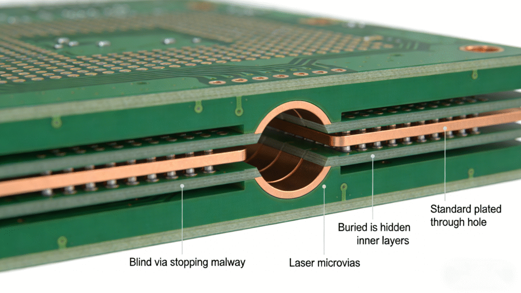
2. The Architecture: Blind and Buried Vias Technology
The true magic of HDI lies in its three-dimensional routing capabilities. Instead of punching a hole completely through the board, Blind and Buried Vias Technology allows connections to be made only where necessary.
- Blind Vias: These connect an outer layer of the PCB to one or more inner layers but do not go all the way through the board. They are “blind” because you can only see them from one side.
- Buried Vias: These connect two or more inner layers and are completely hidden within the substrate. They are invisible from the outside of the board.
- Microvias: Typically laser-drilled, these are tiny holes (often less than 6 mils in diameter) used to connect adjacent layers. In advanced HDI designs, microvias can be stacked or staggered to create complex pathways.
By trapping vias internally or stopping them halfway, engineers free up massive amounts of routing space on the surface and inner planes, allowing for ultra-dense BGA (Ball Grid Array) component placement.
3. Why High-End Industries Demand Microvia PCB Fabrication
Opting for HDI is not merely a design preference; for many cutting-edge sectors, it is a strict requirement. When working with AI hardware, high-end medical equipment, industrial control systems, and new energy vehicles, the margin for error is zero.
These applications demand Microvia PCB Fabrication because it directly impacts reliability. Shorter signal paths reduce electromagnetic interference (EMI) and improve signal integrity in high-frequency applications. Furthermore, the structural density allows medical devices to become implantable or wearable, and enables AI processors to handle massive data throughput without latency.
4. Overcoming Manufacturing Bottlenecks: The Yichao Advantage
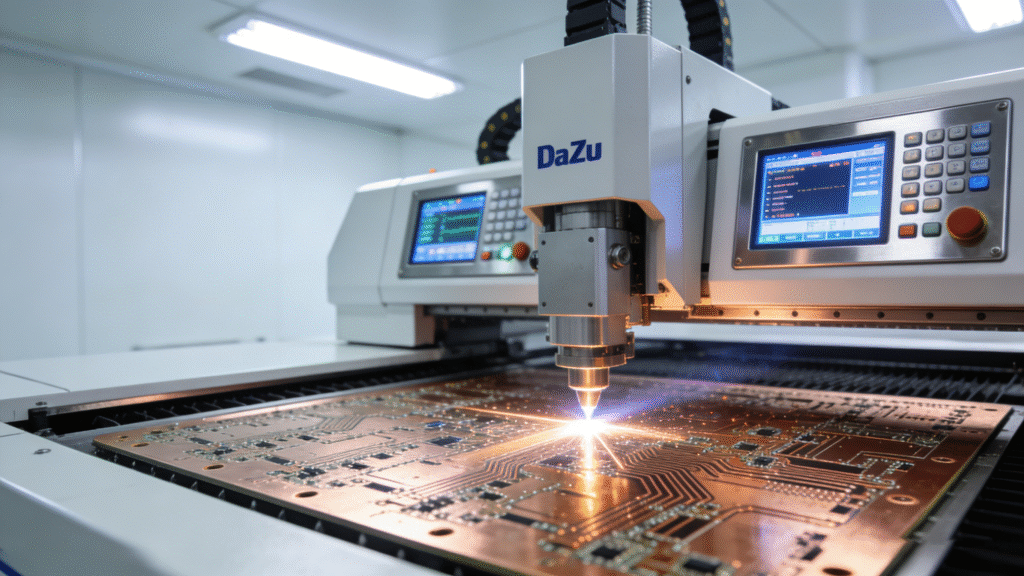
Designing an HDI board is one thing; successfully manufacturing it at scale is another entirely. The precision required to laser-drill microvias and plate them perfectly requires massive capital investment in specialized equipment. This is where partnering with an industry leader becomes critical.
At Yichao Quick Technology, we have evolved into a “specialized, refined, and innovative” enterprise capable of supporting up to 64 layers. Our digital smart factory is equipped to handle the most rigorous HDI requirements. We utilize internationally advanced DaZu six-axis drilling machines and state-of-the-art LDI exposure machines to ensure absolute precision. Whether you specify premium materials from Rogers, Taconic, or Shengyi, our electroplating lines and strict quality control ensure that every microvia is perfectly copper-filled and robust.
5. Securing Your Custom HDI Board Assembly
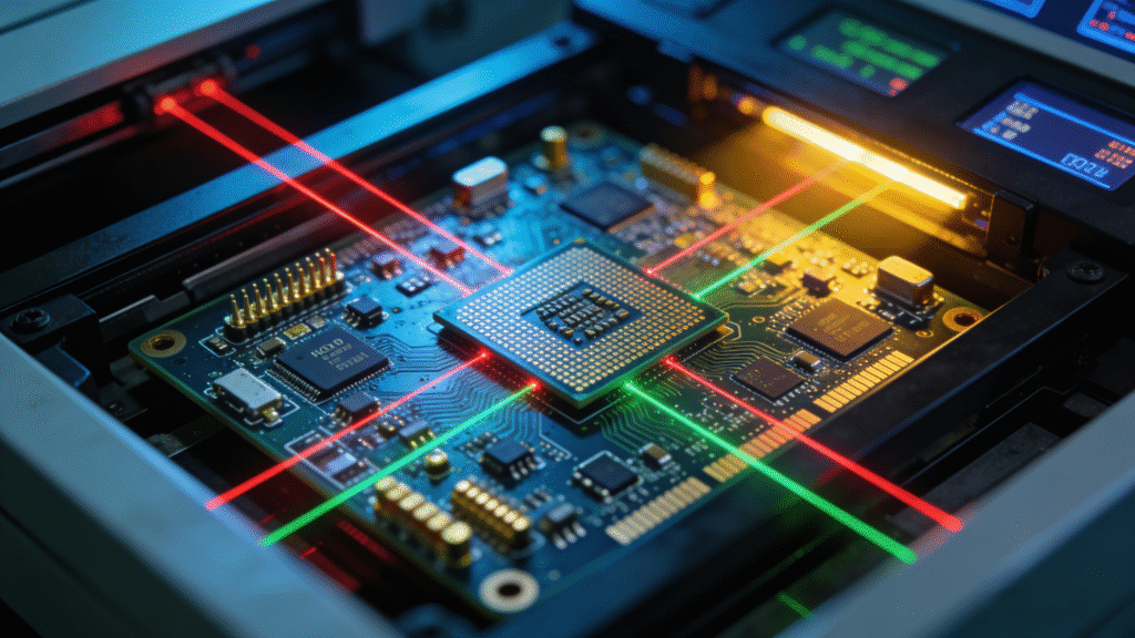
Procuring raw HDI boards is only half the battle. Due to the incredible density of the components—often including extremely fine-pitch BGAs—the Surface Mount Technology (SMT) process must be flawless. Any misalignment during soldering will result in a completely unusable board.
We provide a seamless, one-stop solution for Custom HDI Board Assembly. Our facility operates 25 Yamaha surface mount machines and 4 sets of 10-temperature zone reflow soldering machines, achieving a daily production capacity of 12 million points. Crucially, we validate every HDI assembly utilizing advanced X-RAY testing and AOI (Automated Optical Inspection) to peer beneath the components and guarantee perfectly formed solder joints.
Backed by ISO9001:2015, ISO13485, and IATF16949 certifications, we combine this extreme precision with unparalleled speed—offering 1-minute online ordering and fast shipping to keep your innovation pipeline flowing.
Conclusion
Understanding “What is HDI” is the first step toward unlocking the next tier of electronic product development. By leveraging high-density interconnect technology, you can achieve smaller, faster, and more reliable designs. However, the complexity of HDI requires a manufacturing partner with proven expertise, cutting-edge equipment, and an unyielding commitment to quality. When your design pushes the limits of physics, trust Yichao to bring it to reality.